拓扑绝缘体二维纳米结构与器件
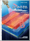
Three-dimensional (3D) topological insulators are a new state of quantum matter that are insulating in the bulk but have current-carrying massless Dirac surface states. Nanostructured topological insulators, such as quasi-two-dimensional (2D) nanoribbons, nanoplates, and ultrathin films with extremely large surface-to-volume ratios, distinct edge/surface effects, and unique physicochemical properties, can have a large impact on fundamental research as wel as in applications such as electronics, spintronics, photonics, and the energy sciences. Few-layer topological insulator nanostructures have very large surface-to-volume ratios that can significantly enhance the contribution of exotic surface states, and their unique quasi-2D geometry also facilitates their integration into functional devices for manipulation and manufacturing. Here, we present our recent results on the control ed growth of quasi-2D nanostructures of topological insulators, as wel as their novel functional devices. High quality quasi-2D nanostructures of Bi2Se3 and Bi2Te3 topological insulators have been synthesized by vapor-phase growth. Ultra-thin nanoplates of the topological insulators with uniform thickness down to a single layer have been grown on various substrates, including conductive graphene. A facile, high-yield method has been developed for growing single-crystal nanoplate arrays of Bi2Se3 and Bi2Te3 with wel-aligned orientations, control ed thickness, and specific placement on mica substrates by van der Waals epitaxy. A systematic spectroscopic study, including angle-resolved photoemission spectroscopy (ARPES), micro-Raman spectroscopy, and micro-infrared spectroscopy, was carried out to investigate the quasi-2D nanostructures of topological insulators. Pronounced Aharonov-Bohm (AB) interference effects were observed in the topological insulator nanoribbons, providing direct transport evidence of the robust, conducting surface states. Transport measurements of a single nanoplate device, with a high-k dielectric top gate, showed a significant decrease in the carrier concentration and a large tuning of the chemical potential with electrical gating. We also present the first experimental demonstration of near-infrared transparent flexible electrodes based on few-layer topological insulator Bi2Se3 nanostructures that was epitaxial y grown on a mica substrate by van der Waals epitaxy. Topological insulator nanostructures show promise as transparent flexible electrodes because of their good near-infrared transparency and excel ent conductivity, which is robust against surface contamination and bending. Our studies suggest that quasi-2D nanostructures of topological insulators show promise for future electronic and optoelectronic applications.
Topological insulator、Dirac fermion、Nanostructure、van der Waals epitaxy、Transparent flexible electrode
O641(物理化学(理论化学)、化学物理学)
2012-11-08(万方平台首次上网日期,不代表论文的发表时间)
共13页
2423-2435


